
aisoc design
DISCLAIMER: This hardware design is provided solely for academic purposes only. It has not undergone formal pre-silicon verification, validation, Emulation, or physical testing, and is not guaranteed for real-world silicon fabrication. The owner / creator accepts no responsibility and/or liability whatsoever for any consequences arising from its use. Use strictly at your own risk.We are going to build a heterogeneous AI accelerator SoC, which consists of 8 NPU Compute Clusters, Distributed tensor/vector processing, a Centralized Scheduler and Command Processor + 1 x high-bandwidth QoS-aware NoC, 4 x HBM4 stacks, 4 x DDR memory, 8 x high-throughput DMA engines, 1 x PCIe/CXL host connectivity, 8 × 100G Ethernet ports. In addition, we will also describe multiple isolated CPU/firmware domains, and system-wide security, power-management, and RAS infrastructure.
Documentation
SoC Specifications
| Parameter | Value | How it is derived |
| NPU clusters / tensor cores | 8 clusters, 32 tensor cores | 4 cores × 128×128 MAC arrays per cluster |
| Peak dense compute | ≈1.89 PFLOPS FP8; ≈0.94 PF BF16; ≈3.77 PF FP4 | 32 × 16,384 MAC × 2 × 1.8 GHz |
| On-chip SRAM | 128 MB cluster scratchpad | 16 MB per cluster, SECDED |
| HBM4 | 4 stacks, 8.19 TB/s, 192 GB | 2048-bit × 8 Gb/s per stack; 48 GB stacks |
| DDR5 | 4 channels DDR5-6400, 204.8 GB/s, ≤ 512 GB | RDIMM, ECC |
| Host interface | PCIe 7.0 x16 / CXL 4.0 Type-2, ≈242 GB/s per direction | 128 GT/s PAM4, FLIT mode |
| Scale-out network | 8 × 100 GbE = 800 Gb/s, RoCEv2 offload | 1 × 112G PAM4 SerDes lane per port |
| DMA | 8 engines, 1.0 TB/s aggregate | 512-bit port at 2 GHz each |
| Control CPUs | 4 isolated domains × 4 RV64 harts | Plus RV32 RoT, PM and scheduler micro-controllers |
| Physical address | 48-bit | 256 TB address space |
| Process / package (assumed) | 3 nm-class, ~800 mm², 2.5D with 4 HBM4 stacks | To be confirmed by physical design |
| TDP envelope | 750 W | Liquid or high-end air cooling |
Block specification summary
| Block | RTL module | Inst. | Clock | Power domain | CSR win. | IRQs | Key figure |
| NPU cluster (SS1) | npu_cluster | 8 | clk_npu[c] 1.8 GHz | PD_NPU0–7 | 2 | 4 each | 236 TFLOPS FP8 each |
| AI datapath (SS2) | ai_datapath | 1 | clk_dp 2.0 GHz | PD_DP | 3 | 4 | 40 × 36, 8.19 TB/s |
| Scheduler (SS3) | scheduler | 1 | clk_noc 2.0 GHz | PD_NOC | 1 | 16 | 64 queues, < 1 µs dispatch |
| NoC (SS4) | noc_top | 1 | clk_noc / clk_cfg | PD_NOC | 0 | 4 | 30 routers, 128 GB/s ports |
| PCIe / CXL (SS5) | pcie_cxl_subsystem | 1 | clk_pcie 1.0 GHz | PD_PCIE | 4 | 16 | x16 128 GT/s |
| Ethernet (SS6) | eth_subsystem / eth_port | 1 / 8 | clk_eth 1.25 GHz | PD_ETH | 5 | 4 / port | 8 × 100 GbE |
| HBM4 (SS7) | hbm_stack | 4 | clk_mem 2.0 GHz | PD_HBM | 6 | 2 each | 2.048 TB/s, 48 GB each |
| DDR5 (SS7) | ddr_subsystem | 1 | clk_mem 2.0 GHz | PD_DDR | 6 | 8 | 4 ch, 204.8 GB/s |
| DMA (SS8) | dma_engine | 8 | clk_noc 2.0 GHz | PD_DMA | 7 | 2 each | 128 GB/s each |
| CPU domain (SS9) | cpu_domain | 4 | clk_cpu[d] 1.0–2.0 GHz | PD_CPU0–3 | 8 | 2 each | 4 RV64 cores each |
| Power mgmt (SS10) | power_mgmt | 1 | clk_aon 100 MHz | AON | 9 | 4 | 20 domains, < 100 ns throttle |
| Security RoT (SS11) | sec_rot | 1 | clk_cfg 500 MHz | AON | 10 | 4 | PQC secure boot |
| RAS (SS11) | ras_aggregator | 1 | clk_cfg 500 MHz | AON | 10 | 8 | 14 sources, ≤ 100 ns fatal |
| Interrupt controller | irq_ctrl | 1 | clk_noc 2.0 GHz | AON | 11 | — | 256 sources, 32 contexts |
| Clock & reset | clock_reset | 1 | ref 100 MHz | AON | 12 | 2 | 6 PLLs, 20 domains |
| Debug & trace | debug_trace | 1 | clk_dbg 250 MHz | PD_DBG | 13 | 4 | 11 trace sources |
NPU / tensor compute cluster (Subsystem 1) – One of eight identical clusters. Each cluster is an independent clock and power domain and receives work from the scheduler.
| Category | Parameter | Specification |
| Identity | RTL module / instances | npu_cluster × 8, inside npu_subsystem |
| Compute | Tensor cores | 4 per cluster; 128 × 128 output-stationary systolic array (16,384 MACs per core) |
| Data formats | FP4, FP6, FP8 (E4M3, E5M2), MXFP4/6/8 block-scaled, BF16, FP16, INT8; FP32 accumulation | |
| Peak throughput per cluster | FP8 / INT8: 236 TFLOPS / TOPS; BF16 / FP16: 118 TFLOPS; FP4: 472 TFLOPS; 2× with 2:4 structured sparsity | |
| Accumulators | 128 × 128 FP32 per core (64 KB register file), double-buffered for back-to-back tiles | |
| Vector unit | 4 lanes × 2048-bit SIMD: 0.92 TFLOPS FP32, 1.84 TFLOPS BF16 (FMA); integer, compare, permute, reduce | |
| Special-function unit | 64 results per cycle (115 G/s): exp, reciprocal, rsqrt, tanh, sigmoid, GELU, log | |
| Memory | Scratchpad SRAM | 16 MB in 32 banks × 512 KB; 512-bit port per bank; ≈3.7 TB/s read (2× the 1.8 TB/s tensor-core demand) |
| Protection | SECDED per 64 bits; scrubbing; ECC errors reported to RAS | |
| Control processor memory | 32 KB I-TCM + 32 KB D-TCM | |
| Data movement | Tile movers | 2 per cluster, each driving 2 datapath ports; up to 5-D strided descriptors; transpose; format conversion |
| Outstanding requests | 64 × 4 KB reads per mover (512 KB per cluster in flight), covering ≈500 ns loaded latency at full rate | |
| Datapath bandwidth | 4 × 256 GB/s = 1.02 TB/s read + 1.02 TB/s write | |
| Control | Control processor | RV32IMAFC (SiFive E76-class), not user-programmable |
| Command interface | 16-entry command FIFO; npu_cmd_t / npu_cpl_t; barrier arrive | |
| Clocking | Core clock | clk_npu[c]: 1.8 GHz nominal, 0.6–2.2 GHz DVFS (from NPU PLL A or B) |
| Port clocks | Datapath and C2C ports on clk_dp; NoC and command ports on clk_noc; CSR on clk_cfg; PM on clk_aon | |
| Power | Domain / states | PD_NPU0–7; OFF, RETENTION (SRAM retained), IDLE, LOW, NOMINAL, TURBO |
| Throttle | throttle_t input: 8 levels; fast droop throttle within 100 ns | |
| Interfaces | AI datapath | 4 × AXI4 1024-bit managers (dp_req/rsp) |
| System NoC | 1 × AXI4 512-bit manager; 1 × AXI4 512-bit subordinate (SRAM window, 16 MB in a 256 MB slot) | |
| C2C ring | 512-bit flit TX and RX with ready | |
| RAS | Features | SECDED on SRAM and accumulator RF; parity on pipelines; poison consumption aborts the job only; ERR_INJECT |
| Registers / IRQ | CSR window / interrupts | Window 2, 1 MB per cluster; 4 interrupt lines per cluster |
| IP | Source | In-house tensor cores, vector unit, movers; licensed control core; foundry memory compilers |
| Budget | Area / power per cluster | 52 mm² / 50 W at FP8 full load (≈4.7 TFLOPS/W) |
AI Fabric (Subsystem 2) – Dedicated memory fabric between the clusters and HBM/DDR, sized to carry the full HBM bandwidth.
| Category | Parameter | Specification |
| Identity | RTL module | ai_datapath |
| Ports | Initiators | 40: 32 NPU AXI4 1024-bit + 8 NoC AXI4 512-bit (up-sized to 1024-bit with async width converters) |
| Targets | 36: 32 HBM AXI4 1024-bit + 4 DDR AXI4 512-bit | |
| Topology | Quadrant switches | 4 (one per HBM stack); each 13 × 12 crossbar: 10 local initiators + 3 mesh inputs, 9 local targets + 3 mesh outputs |
| Inter-quadrant mesh | 6 bidirectional links (full mesh); 3 × 1024-bit lanes per direction per link = 768 GB/s; 9.2 TB/s aggregate | |
| Mesh headroom | 1.5× the 6.1 TB/s that uniform hashing sends across quadrants | |
| Performance | Peak bandwidth | 8.19 TB/s NPU ↔ HBM; 1.02 TB/s NoC ↔ memory |
| Zero-load latency (one way) | ≤ 4 ns quadrant-local; ≤ 10 ns via mesh | |
| Outstanding | Per NPU port 64 reads + 32 writes; per NoC port 128 reads + 64 writes | |
| Addressing | HBM interleave | All 32 ports; default 256 B granule with XOR hash; selectable 4 KB, 2 MB, or NUMA (home quadrant) |
| DDR interleave | 4 channels at 4 KB | |
| QoS | Regulation | 40 token-bucket regulators (1 GB/s granularity); 4 priority levels from AxQOS; age escalation |
| DRAM efficiency | Read/write batching with programmable watermarks toward HBM | |
| C2C ring | Configuration | 8 nodes, bidirectional, 512-bit at 2 GHz: 128 GB/s per hop per direction; 2 virtual channels; credit-based |
| Latency / protection | 2 ns per hop; CRC with link-level retry | |
| Clocking / power | Clock / domain | clk_dp 2.0 GHz (fixed); PD_DP, gated only when all HBM is idle |
| RAS | Features | ECC sideband on every beat; poison propagation in axi_user_t; write-data parity; response timeouts |
| Registers / IRQ | CSR window / interrupts | Window 3; 4 interrupt lines |
| IP | Source | Arteris FlexNoC 5 (FlexGen) for switches; in-house hash, regulators and C2C ring |
| Budget | Area / power | 30 mm² / 25 W |
Scheduler / command processor (Subsystem 3)
| Category | Parameter | Specification |
| Identity | RTL module | scheduler |
| Queues | Host submission queues | 64 ring buffers (host or device memory), up to 64K entries each; one 4 KB doorbell page per queue at CSR +8 MB, mappable to a VF |
| Hardware run-queues | 16, with 4 priority levels | |
| Tenants | 16 tenant contexts; weighted fair share; per-tenant cluster masks | |
| Execution contexts | 4,096 (12-bit ctx_id in npu_cmd_t) | |
| Dispatch | Rate | Up to 1 command per cluster per cycle at 2 GHz; sustained ≥ 100 M commands/s |
| Latency | Doorbell to first dispatch < 1 µs for device-memory queues | |
| Targets | 8 NPU clusters (npu_cmd_t) and 8 DMA engines (dma_cmd_t) | |
| Synchronization | Hardware barriers | 64 barriers / counting semaphores |
| Fences | 64-bit timeline values written to memory; host-visible | |
| Preemption | Modes | Cooperative at tile boundaries; forced after programmable timeout (1 µs – 1 s) |
| Control | Micro-controller | RV32IMAFC (SiFive E76-class), 64 KB I-TCM + 64 KB D-TCM; handles exceptional commands |
| Queue state SRAM | 512 KB, SECDED | |
| Clocking / power | Clock / domain | clk_noc 2.0 GHz; PD_NOC (system functional, not gated) |
| Interfaces | Buses and sideband | 1 × AXI4 512-bit NoC manager; 8 × command / completion; barrier arrive / release; 8 × DMA command / completion; throttle input |
| RAS | Features | Command watchdog per cluster; ECC on queue SRAM; errors to RAS |
| Registers / IRQ | CSR window / interrupts | Window 1 (doorbells at +8 MB); 16 interrupt lines |
| IP | Source | In-house dispatch engine; licensed micro-controller; DesignWare timers and watchdog |
| Budget | Area / power | 4 mm² / 2 W |
NoC / interconnect (Subsystem 4)
| Category | Parameter | Specification |
| Identity | RTL module | noc_top |
| Data NoC | Topology | 6 × 5 2D mesh, 30 routers, XY routing; separate request and response networks |
| Links | 512-bit at 2.0 GHz: 128 GB/s per port per direction | |
| Router | 2-cycle pipeline; 4 virtual channels × 8-flit buffers per input | |
| Latency | ≈1.5 ns per hop; ≤ 15 ns corner to corner at zero load | |
| Bisection | ≈1.5 TB/s per physical network | |
| Ports | Initiator NIs | 27: PCIe 2, Ethernet 2, DMA 8, CPU 4, NPU 8, scheduler 1, debug 1, security 1 |
| Target NIs | 23: AI-datapath memory 8, PCIe outbound 2, NPU SRAM 8, CPU SRAM 4, security mailbox 1 | |
| Protocol | AXI4, 48-bit address, 12-bit ID after remap, 16-bit user (axi_user_t); 64 outstanding per NI | |
| QoS | Traffic classes | TC0 control (strict, capped), TC1 latency (WRR high), TC2 bulk (WRR + token buckets), TC3 network (≥ 100 GB/s reserved) |
| Security | Firewalls | Per target NI: 16 regions, 16-bit domain allow mask, secure attribute; locked by RoT (fw_cfg_lock) |
| Identity stamping | Domain, tenant, secure and TC stamped by initiator NIs in hardware | |
| RAS | Timeouts | Per target NI, programmable 1 µs – 100 ms; returns SLVERR and reports to RAS |
| Config NoC | Structure | AXI → APB bridge; APB4 32-bit tree at 500 MHz (clk_cfg); 14 ports, 16 MB window each |
| Clocking / power | Clock / domain | clk_noc 2.0 GHz (1.0–2.0 GHz); PD_NOC, never power-gated, idle routers clock-gated |
| Observability | Probes | Per-link bandwidth, VC occupancy and latency counters; feeds debug trace |
| Registers / IRQ | CSR window / interrupts | Window 0; 4 interrupt lines |
| IP | Source | Arteris FlexNoC 5 with FlexGen; FlexNoC Resilience Package |
| Budget | Area / power | 25 mm² / 15 W |
PCIe / CXL (Subsystem 5)
| Category | Parameter | Specification |
| Identity | RTL module | pcie_cxl_subsystem |
| Link | Standard / rate | PCIe 7.0, 128 GT/s PAM4, FLIT mode; backward compatible to Gen 1 |
| Width | x16; bifurcation x16, 2 × x8, 4 × x4 | |
| Bandwidth | 256 GB/s raw, ≈242 GB/s effective per direction | |
| CXL | Device type | CXL 4.0 Type-2: CXL.io, CXL.cache, CXL.mem |
| Coherency | Device coherency engine (DCOH) with 4 MB snoop filter | |
| Memory exposure | HBM + DDR (up to 704 GB) as host-managed device memory; 4 HDM decoders | |
| Virtualization | Functions | SR-IOV: 1 PF + 63 VFs; FLR per function |
| Address translation | ATS with 2,048-entry device TLB; PRI | |
| Interrupts | MSI-X, 2,048 vectors across PF and VFs | |
| Security | Link encryption | IDE (AES-256-GCM): link IDE and up to 8 selective IDE streams; keys from RoT key bus |
| Attestation / TEE | DOE mailbox; SPDM 1.3 responder; TDISP for confidential device assignment | |
| Power | States | Link L0, L0p, L1, L1.2; device D0, D3hot, D3cold; PD_PCIE |
| Clocking | Clocks | pcie_refclk 100 MHz; controller clk_pcie 1.0 GHz; PIPE to PHY |
| Interfaces | NoC | 2 × AXI4 512-bit managers (inbound), 2 × AXI4 512-bit subordinates (outbound) = 256 GB/s per direction |
| Sideband | msi_req_t from interrupt controller; host_err_t (AER) from RAS; PERST#, CLKREQ#, WAKE# | |
| Timing | Boot | Link training complete < 100 ms after PERST# deassertion (from ROM defaults) |
| RAS | Features | LCRC / FLIT CRC with replay; AER correctable, non-fatal, fatal |
| Registers / IRQ | CSR window / interrupts | Window 4; 16 interrupt lines |
| IP | Source | Synopsys PCIe 7.0 controller with CXL 4.0, PCIe 7.0 PHY, IDE security module |
| Budget | Area / power | 23 mm² / 12 W |
100G Ethernet × 8 (Subsystem 6)
| Category | Parameter | Specification |
| Identity | RTL module | eth_subsystem with eth_port × 8 |
| PHY | Ports / lanes | 8 × 100GBASE-KR1 / CR1, one 112G PAM4 SerDes lane each (106.25 Gb/s line rate) |
| Ganging | 2 × 400G or 4 × 200G | |
| FEC | RS(544,514) | |
| MAC | Features | IEEE 802.3; frames up to 9,216 B; PFC (8 priorities); ETS; IEEE 1588 PTP one- and two-step timestamping |
| RDMA | Transport | RoCEv2 offload: Send/Receive, Write, Read, Atomics; reliable connected and unreliable datagram |
| Scale | 16K queue pairs; programmable congestion control (DCQCN-compatible) | |
| Latency target | < 2 µs one-way RDMA write chip to chip through one switch | |
| Collectives | Engine | All-reduce, reduce-scatter, all-gather, broadcast; ring and tree algorithms; FP32 / BF16 / FP8 reductions in-line |
| Buffering | Packet buffer | 8 MB shared, ECC |
| Security | Encryption | MACsec and PSP at line rate (AES-GCM-256); keys from RoT key bus |
| Bandwidth | Aggregate | 800 Gb/s = 100 GB/s per direction |
| Clocking / power | Clock / domain | eth_refclk 156.25 MHz; clk_eth 1.25 GHz; PD_ETH with per-port gating |
| Interfaces | NoC | 2 × AXI4 512-bit managers on TC3 (256 GB/s) |
| Module management | Shared I²C; per-port presence, interrupt, reset, low-power pins | |
| Registers / IRQ | CSR window / interrupts | Window 5: 1 MB per port + engine; 4 interrupt lines per port (32) |
| IP | Source | Synopsys 112G PHY, 800G PCS, 100–800G MAC, MACsec; in-house RDMA and collective engine |
| Budget | Area / power | 22 mm² / 15 W |
HBM4 memory (Subsystem 7) – Specification per stack; the SoC has four.
| Category | Parameter | Specification |
| Identity | RTL module | hbm_stack × 4, inside memory_subsystem |
| Device | Standard | JEDEC JESD270-4 (HBM4) |
| Capacity | 48 GB per stack (16-high, 24 Gb dies); 192 GB total | |
| Interface | 2048 DQ: 32 channels × 64 DQ, 2 pseudo-channels per channel (64 per stack) | |
| Data rate | 8 Gb/s per pin → 2.048 TB/s per stack, 8.19 TB/s total | |
| Controller | Host ports | 8 × AXI4 1024-bit (256 GB/s each), each serving 4 channels |
| Scheduling | Out-of-order FR-FCFS, bank-group aware; 64-entry read and 64-entry write queue per channel; write-drain watermarks | |
| Refresh | All-bank and per-bank refresh; refresh management (RFM); temperature-compensated | |
| PHY interface | DFI 5.x | |
| Performance | Zero-load read latency | ≤ 60 ns at the controller port (row miss) |
| Efficiency | ≥ 85% of peak for streaming reads; ≥ 75% for mixed 2:1 read/write random 256 B | |
| RAS | Features | On-die ECC + controller ECC on ECC pins; error check and scrub (ECS); soft and hard post-package repair; poison on uncorrectable |
| Thermal | Monitoring | 3-bit temperature and catastrophic trip per stack to power management |
| Test | Access | IEEE 1500 wrapper per stack; PHY BIST and loopback |
| Clocking / power | Clock / domain | clk_mem 2.0 GHz controller; host ports on clk_dp; PD_HBM; self-refresh in RETENTION and OFF |
| Registers / IRQ | CSR window / interrupts | Window 6, 2 MB per stack; 2 interrupt lines per stack |
| IP | Source | Rambus HBM4 controller; Synopsys or Cadence HBM4 PHY |
| Budget | Area / power | 24 mm² per stack (PHY 18 + controller 6) / 8 W PHY + controller; DRAM stack ≈30 W in package |
DDR5 memory (Subsystem 7)
| Category | Parameter | Specification |
| Identity | RTL module | ddr_subsystem, inside memory_subsystem |
| Device | Standard / speed | JEDEC JESD79-5 DDR5-6400 RDIMM, 1 DIMM per channel |
| Channels | 4; each 2 sub-channels × 40 bit (32 data + 8 ECC) | |
| Capacity | Up to 128 GB per channel, 512 GB total | |
| Performance | Bandwidth | 204.8 GB/s peak; ≥ 174 GB/s sustained |
| Zero-load read latency | ≤ 90 ns at the controller port | |
| Controller | Host ports | 4 × AXI4 512-bit (one per channel) on clk_dp |
| Scheduling | FR-FCFS, 64-entry queues per channel | |
| PHY interface | DFI 5.x; training (write leveling, read and write centering, Vref) run by CPU D0 | |
| RAS | Features | SDDC-class (x4 chipkill) ECC; on-die ECC; patrol scrub; post-package repair; alert handling |
| Security | Inline encryption | AES-XTS-256 at line rate; 16 key slots (per tenant) from RoT key bus |
| Clocking / power | Clock / domain | clk_mem 2.0 GHz; PD_DDR; self-refresh in RETENTION and OFF |
| Registers / IRQ | CSR window / interrupts | Window 6 at +8 MB; 8 interrupt lines (2 per channel) |
| IP | Source | Synopsys DDR5 controller and PHY; Synopsys inline memory encryption module |
| Budget | Area / power | 16 mm² / 8 W |
DMA engine (Subsystem 8) – Specification per engine; the SoC has eight.
| Category | Parameter | Specification |
| Identity | RTL module | dma_engine × 8, inside dma_subsystem |
| Bandwidth | Per engine / total | 128 GB/s (512-bit at 2 GHz) / 1.02 TB/s |
| Channels | Count / arbitration | 16 per engine (128 total); priority + weighted round-robin |
| Descriptors | Formats | Linear, 2-D, 3-D strided, scatter-gather linked list; up to 4 GB per descriptor |
| Sources of work | CSR doorbell (CPU) or dma_cmd_t from the scheduler | |
| Latency tolerance | Outstanding reads | 128 reads up to 4 KB each (512 KB in flight), covering ≈4 µs at full rate — enough for PCIe host reads |
| Reorder buffer | 256 KB, ECC | |
| Transforms | In-flight operations | FP32 ↔ BF16 / FP16 / FP8 conversion; CRC32C; fill pattern |
| Completion | Reporting | dma_cpl_t to scheduler and / or 2 interrupt lines per engine |
| Clocking / power | Clock / domain | clk_noc 2.0 GHz; PD_DMA |
| QoS | Traffic class | TC2 bulk, limited by NoC token buckets |
| Registers / IRQ | CSR window / interrupts | Window 7, 1 MB per engine; 2 interrupt lines per engine |
| IP | Source | In-house |
| Budget | Area / power | 1 mm² / 0.6 W per engine (8 mm² / 5 W total) |
CPU / firmware domain (Subsystem 9) – Specification per domain; the SoC has four isolated domains.
| Category | Parameter | Specification |
| Identity | RTL module | cpu_domain × 4, inside cpu_subsystem |
| Roles | D0 / D1 / D2 / D3 | System management and RAS / runtime / network control plane / host interface |
| Cores | D0 | 4 × RV64GC in-order (SiFive P550-class); cores 0–1 can run as a dual-core lockstep pair |
| D1–D3 | 4 × RV64GCV out-of-order with vector (SiFive P870-class) | |
| Frequency | D0 1.0 GHz; D1–D3 2.0 GHz with DVFS | |
| Memory | Caches | Private L1 instruction and data caches per core; 2 MB shared L2 per domain, ECC |
| Tightly coupled SRAM | 1 MB per domain, visible in the CPU SRAM window (16 MB slot per domain) | |
| Protection / translation | PMP and Smepmp; Sv39 / Sv48 MMU on D1–D3 (Linux-capable); D0 runs an RTOS | |
| Interrupts | Inputs | RISC-V AIA: IMSIC per core (M and S files), external MEIP / SEIP, NMI from RAS |
| Isolation | Mechanisms | Separate clock, reset, power domain and NoC domain ID; inter-domain traffic only through 4 hardware mailboxes per domain |
| Debug | Access | RISC-V Debug 1.0 via DMI from debug_trace, gated by dbg_auth_t |
| Safety | Watchdog | 1 per domain, reports to RAS |
| Boot | Release | Held in reset until the RoT verifies the image and asserts cpu_rel[d]; boot vector from RoT |
| Interfaces | NoC | 1 × AXI4 512-bit manager; 1 × AXI4 512-bit subordinate (TCM window) |
| D0 peripherals | UART console, 16 GPIO | |
| Clocking / power | Clock / domain | clk_cpu[d]; PD_CPU0–3 (D0 never gated; D1–D3 gateable with L2 retention) |
| Registers / IRQ | CSR window / interrupts | Window 8, 4 MB per domain; 2 mailbox interrupt lines per domain |
| IP | Source | SiFive Performance P870 and P550; DesignWare UART and GPIO; in-house mailboxes and lockstep wrapper |
| Budget | Area / power | 6 mm² / 5 W per domain (24 mm² / 20 W total) |
Power management (Subsystem 10)
| Category | Parameter | Specification |
| Identity | RTL module | power_mgmt |
| Controller | Processor | RV32IMAFC (SiFive E76-class), 64 KB I-TCM + 64 KB D-TCM; firmware verified by the RoT |
| Domains | Power domains | 20 gateable domains (pd_e) plus the always-on domain |
| P-states | OFF, RETENTION, IDLE, LOW, NOMINAL, TURBO via pm_req_t / pm_rsp_t handshake | |
| Transition targets | IDLE ↔ NOMINAL < 1 µs (clock gating); RETENTION ↔ NOMINAL < 50 µs; OFF ↔ NOMINAL < 1 ms | |
| DVFS | Frequency control | clk_ctrl_t per clock domain (enable, PLL select, divider); NPU 0.6–2.2 GHz, CPU 1.0–2.0 GHz |
| Voltage control | AVS over PMBus to board regulators, per rail | |
| Sensing | On-die sensors | 64 thermal sensors (±1 °C after calibration); 32 voltage-droop detectors; 8 process monitors |
| External | HBM temperature and catastrophic trip per stack | |
| Control loops | TDP loop | ≈1 ms period; activity-based power estimate per domain |
| Fast throttle | Droop or di/dt event to cluster throttle in < 100 ns | |
| Thermal trip | Hardware thermtrip_n at 125 °C, independent of firmware | |
| Telemetry | Reporting | Per-domain power and temperature at 1 kHz, reported to host through CPU D3 |
| Clocking / power | Clock / domain | clk_aon 100 MHz; always-on domain |
| Registers / IRQ | CSR window / interrupts | Window 9; 4 interrupt lines |
| IP | Source | SiFive E76-class controller; Synopsys SLM PVT monitors; DesignWare I²C (PMBus) |
| Budget | Area / power | 2 mm² / 0.5 W |
Security root of trust (Subsystem 11)
| Category | Parameter | Specification |
| Identity | RTL module | sec_rot, inside security_ras |
| Processor | Core / memory | RV32 RoT core; boot ROM (1 MB window); 1 MB secure SRAM; private to the RoT |
| Storage | OTP | 16 KB: root keys, lifecycle state, anti-rollback counters, repair data |
| Boot flash | QSPI, A/B firmware images | |
| Crypto | Symmetric / hash | AES-256 (GCM, XTS, CTR); SHA-2 and SHA-3; HMAC; KDF (NIST SP 800-108) |
| Public key | ECDSA P-384; ML-DSA-87 and ML-KEM-1024 (FIPS 204 / 203) | |
| Random numbers | TRNG with SP 800-90B health tests; DRBG | |
| Boot | Secure and measured boot | Dual signatures (ECDSA-P384 + ML-DSA-87) on every image; measurements recorded for attestation |
| Attestation | Protocol | SPDM 1.3 responder via PCIe DOE; DICE-based device identity |
| Keys | Key bus | Side-loaded keys to PCIe IDE, Ethernet MACsec / PSP and DDR encryption; never visible to software |
| Lifecycle | States | RAW, TEST, DEV, PROD, RMA, SCRAP; gates debug and test features |
| Isolation | Controls | cpu_rel and boot vectors per domain; NoC firewall lock; debug authorization (dbg_auth_t) |
| Tamper | Detection | Voltage and clock glitch detectors |
| Certification | Target | Designed for FIPS 140-3 validation |
| Clocking / power | Clock / domain | clk_cfg 500 MHz; always-on domain |
| Registers / IRQ | CSR window / interrupts | Window 10 (+0); 4 interrupt lines |
| IP | Source | Rambus RT-6xx Root of Trust; Rambus Quantum Safe Engine; Synopsys NVM OTP |
| Budget | Area / power | 3 mm² / 0.5 W |
Error management / RAS (Subsystem 11)
| Category | Parameter | Specification |
| Identity | RTL module | ras_aggregator, inside security_ras |
| Inputs | Error sources | 14 (one ras_err_t per top-level block): corrected, deferred, uncorrected, fatal + 8-bit code |
| Records | Format | Per-source error records in RISC-V RERI layout: status, address, syndrome, 64-bit timestamp |
| Retention | Preserved across warm reset (always-on and configuration domains) | |
| Policy | Thresholds | Per-source corrected-error thresholds and leaky-bucket storm detection |
| Escalation | Interrupt → NMI to all domains → host AER → fault_n pin → optional warm reset | |
| Timing | Targets | Fatal to NMI ≤ 50 ns; fatal to fault_n ≤ 100 ns |
| Validation | Injection | Error injection in every block through the common ERR_INJECT register |
| Clocking / power | Clock / domain | clk_cfg 500 MHz; always-on domain |
| Registers / IRQ | CSR window / interrupts | Window 10 (+8 MB); 8 interrupt lines |
| IP | Source | In-house |
| Budget | Area / power | 1 mm² / 0.5 W |
Interrupt controller
| Category | Parameter | Specification |
| Identity | RTL module | irq_ctrl |
| Wired interrupts | APLIC | 256 level-sensitive sources (166 used); 2-flop synchronizers; 7 priority levels |
| Contexts | 32: 4 domains × 4 cores × machine and supervisor | |
| Message interrupts | IMSIC | Per core, machine and supervisor files, 255 identities each |
| Host interrupts | MSI-X generator | 2,048 vectors, tagged with PF / VF index |
| Latency | Targets | Source to core ≤ 20 ns; scheduler completion to MSI-X on the link ≤ 300 ns |
| Security | Routing lock | Source-to-domain routing set by secure firmware and locked |
| Clocking / power | Clock / domain | clk_noc 2.0 GHz; always-on domain |
| Registers | CSR window | Window 11 |
| IP | Source | In-house, RISC-V AIA 1.0 compliant |
| Budget | Area / power | 1 mm² / 0.5 W |
Clock and reset
| Category | Parameter | Specification |
| Identity | RTL module | clock_reset (with rst_sync, clk_gate) |
| References | Inputs | ref_clk_100m; pcie_refclk 100 MHz; eth_refclk 156.25 MHz |
| PLLs | Count / type | 6: SYS (4.0 GHz VCO), NPU A, NPU B, CPU, MEM, plus PHY-internal PLLs; fractional-N; lock < 50 µs |
| Distribution | Domains | 20 clock domains (clk_e); divider 1–16, glitch-free mux and ICG per domain |
| Monitoring | Clock monitor on every PLL output: loss of lock and frequency deviation > 1% → RAS | |
| Reset | Structure | 20 domain resets; asynchronous assert, synchronous de-assert through 3-stage synchronizers |
| Sequencing | POR → AON + RoT → PLLs → fabrics → CPU domains on cpu_rel; warm reset from RAS preserves AON and CFG | |
| DFT | Test controls | Clock-gate override and reset-synchronizer bypass in test mode |
| Clocking / power | Domain | Always-on |
| Registers / IRQ | CSR window / interrupts | Window 12; 2 interrupt lines (PLL unlock, clock-monitor fault) |
| IP | Source | Analog Bits PLLs; in-house sequencer and monitors |
| Budget | Area / power | 3 mm² / 2 W |
Debug, trace and DFT
| Category | Parameter | Specification |
| Identity | RTL module | debug_trace |
| Debug access | JTAG | IEEE 1149.1 TAP; IEEE 1687 (IJTAG) network; RISC-V DTM → DMI to the 4 CPU domains |
| Authorization | dbg_auth_t from RoT (invasive, non-invasive, secure); lifecycle-gated | |
| Trace | Sources / funnel | 11 sources × 64-bit trace (trc_e); funnel with per-source IDs |
| Storage | 64 KB on-chip trace buffer; trace router spills to DDR (up to 4 GB) over a NoC manager | |
| Cross-trigger | 8 channels across all 14 blocks | |
| Timestamp | Global 64-bit counter on clk_aon, broadcast to all blocks | |
| DFT | Scan | Compressed scan; targets ≥ 99% stuck-at, ≥ 95% transition-fault coverage |
| Memory test | MBIST with repair for all SRAMs (128 MB scratchpad included) | |
| PHY test | SerDes loopback and PRBS; HBM IEEE 1500 and BIST; DDR PHY BIST | |
| Clocking / power | Clock / domain | clk_dbg 250 MHz; PD_DBG |
| Registers / IRQ | CSR window / interrupts | Window 13; 4 interrupt lines |
| IP | Source | Siemens Tessent Embedded Analytics, IJTAG and MBIST; Synopsys TestMAX (alternative) |
| Budget | Area / power | 4 mm² / 1 W |
Area and power budget – Each block team designs to the allocation below. The logic die must stay under the reticle limit with margin for floorplan whitespace, and the package must stay inside the 750 W TDP with a margin for estimation error and voltage-regulation effects.
| Block | Instances | Area each (mm²) | Area total (mm²) | Power total (W) | Share of die area |
| NPU cluster | 8 | 52 | 416 | 400 | 53% |
| HBM4 controller + PHY | 4 | 24 | 96 | 32 | 12% |
| AI datapath | 1 | 30 | 30 | 25 | 4% |
| NoC (data + config) | 1 | 25 | 25 | 15 | 3% |
| CPU domains | 4 | 6 | 24 | 20 | 3% |
| PCIe / CXL | 1 | 23 | 23 | 12 | 3% |
| Ethernet ×8 | 1 | 22 | 22 | 15 | 3% |
| DDR5 controller + PHY | 1 | 16 | 16 | 8 | 2% |
| DMA | 8 | 1 | 8 | 5 | 1% |
| Scheduler | 1 | 4 | 4 | 2 | 0.5% |
| Security RoT + RAS | 1 | 4 | 4 | 1 | 0.5% |
| Debug and trace | 1 | 4 | 4 | 1 | 0.5% |
| Clock and reset | 1 | 3 | 3 | 2 | < 1% |
| Power management | 1 | 2 | 2 | 0.5 | < 1% |
| Interrupt controller | 1 | 1 | 1 | 0.5 | < 1% |
| Top-level routing, DFT, I/O, whitespace | — | — | 102 | 3 | 13% |
| Logic die total | 780 | 542 | 100% | ||
| HBM4 DRAM stacks (in package) | 4 | — | — | 120 | — |
| Package total | 662 | ||||
| Margin to 750 W TDP | 88 (12%) |
SoC Overview
The SoC is a data-center accelerator card ASIC for large-model AI. It targets three workload classes: training of large transformer models (compute and network bound), inference prefill (compute bound) and inference decode (memory-bandwidth bound). The architecture therefore balances raw tensor throughput with very high HBM bandwidth, a dedicated memory fabric, low-latency collectives inside the chip, and an 800 Gb/s scale-out network between chips.
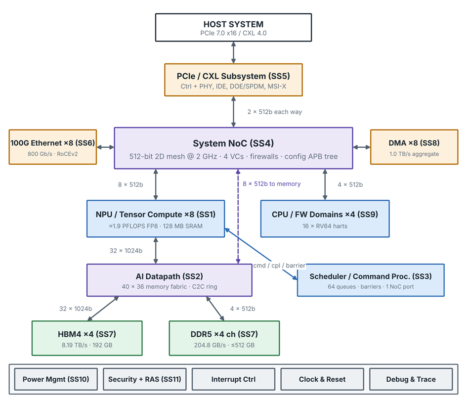
Two separate fabrics carry data. The System NoC carries control, host, DMA and network traffic between all subsystems. The AI Datapath is a dedicated high-bandwidth memory fabric between the NPU clusters and HBM/DDR, so that bulk tensor traffic never competes with control or host traffic. The NoC reaches memory through eight ports into the AI Fabric (ai_datapath).
Subsystem Summary
| # | Subsystem | Primary function | Principal IP |
| 1 | NPU / Tensor Compute | Matrix and vector compute, 8 clusters | In-house tensor cores; SiFive E-series control cores |
| 2 | AI Datapath | Compute-to-memory fabric, collective ring | Arteris FlexNoC 5 / in-house crossbar |
| 3 | Scheduler / Command Processor | Host queues, dispatch, synchronization | In-house dispatch engine; SiFive E76 µC |
| 4 | NoC / Interconnect | System data network and CSR network | Arteris FlexNoC 5 with FlexGen |
| 5 | PCIe / CXL | Host link, CXL.mem/.cache, MSI-X | Synopsys PCIe 7.0 + CXL 4.0 controller and PHY |
| 6 | 100G Ethernet ×8 | Scale-out network, RDMA | Synopsys 112G PHY, 800G MAC/PCS |
| 7 | HBM / DDR Memory | HBM4 and DDR5 controllers and PHYs | Rambus HBM4 controller; Synopsys DDR5 |
| 8 | DMA | Bulk data movement | In-house engines |
| 9 | CPU / Firmware Domains | Management and runtime firmware | SiFive P870 / P550 |
| 10 | Power Management | DVFS, power gating, thermal | SiFive E-series; Synopsys SLM PVT monitors |
| 11 | Security + RAS | Root of trust, keys, error management | Rambus RT-6xx Root of Trust |
End-to-end command flow
The following sequence shows how a unit of AI work travels through the chip; it is the main use case the architecture is optimized for.
– The host writes command buffers to host or device memory and rings a doorbell (a write to the scheduler’s doorbell page through PCIe and the NoC).
– The scheduler fetches the command descriptors, resolves dependencies (barriers and semaphores) and applies tenant QoS.
– The scheduler dispatches commands to one or more NPU clusters over dedicated sideband links, and kicks DMA engines for host transfers.
– Clusters stream weights and activations from HBM through the AI datapath into their SRAM, compute, and exchange partial results over the C2C ring; cross-chip collectives go out through the Ethernet RDMA engine.
– Clusters return completions; the scheduler writes a completion record and fence value to memory.
– The interrupt controller sends an MSI-X to the host, which retires the work.
IP Strategy
The program licenses standards-based IP where the standard defines the behaviour and silicon-proven PHYs carry high risk (PCIe, CXL, Ethernet, HBM, DDR, root of trust, NoC generation tooling, RISC-V CPU cores). It develops in-house the blocks that differentiate the product: tensor cores, vector units, the AI datapath’s hashing and QoS, the scheduler dispatch engine, the high-throughput DMA engines, the collective ring and the RDMA/collective offload engine.
| Criterion | Licensed IP | In-house IP |
| Standard defines behaviour | Preferred (compliance, interop) | Avoid |
| Mixed-signal / SerDes / PHY | Required | Not planned |
| Product differentiation | Avoid | Preferred |
| Schedule risk | Lower for proven IP | Higher; mitigated by early RTL shells |
- Subsystem Overview, PLL’s, Monitors, Debug & Trace, JTAG & DFT.
- Global Interrupt, Clocking, Reset Architecture
- Address Map